Sections
Nantenna also known as nano antenna is a rectifying antenna which is nanoscopic. This is used to convert light to electric power. It works based on the rectifying antenna, a commonly used device in wireless power transmission. The function of rectenna is to convert the radio waves to the form of current electricity. We all know that light composes of EM waves of small wavelength.
Nantenna can be defined as a small rectenna which is small in size of a light wave. Its fabrication is done using nanotechnology. Nantenna acts as an antenna which helps in the conversion of light to current electricity. These are said to be the most efficient means to produce the solar power and also considered to be more efficient than the solar cells. The idea of Nantenna was first developed by Robert. L. Bailey in the year of 1972.
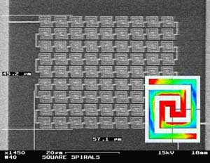
Idaho National Laboratories designed a nantenna which was used to absorb the wavelengths in the range of 3-15µm. The corresponding photon energy is 0.08-0.4 electron volt. Depending on the antenna theory, nantenna absorbs the wavelength of light efficiently providing the size of the nantenna is optimized for the specific wavelength.
|
Year |
Name |
Explanation |
|
1973 |
Robert Bailey, James C. Fletcher |
Electromagnetic wave converter |
|
1974 |
T. Gustafson |
Rectify even visible light to DC current |
|
1996 |
Guang H. Lin |
Resonant light absorption by a fabricated nanostructure and light rectification with frequencies in visible range. |
|
2002 |
ITN Energy Systems |
Optical antennas coupled with high frequency diodes |
|
2015 |
|
Solar energy collector that can convert optical light to DC current |

Figure 1: Nanantenna

Figure 2: Nanantenna Solar Sheet
Lithography Method
A metallic ground plane is placed to the silicon wafer. After this, sputter deposition of amorphous silicon layer is placed. For the antenna, a thin manganese film along with the gold frequency selective is deposited. Resist was applied and later on patterned using the electron beam lithography. Later on the gold film is etched and the resist is being removed.
Roll to Roll Manufacturing
Roll to roll manufacturing method is being used based on the master pattern. The master pattern mechanically stamps the pattern on the inexpensive flexible substrate and helps in creating the metallic loop elements.
Sections