Sections
Transparent or invisible electronics is one of the leading forms of technology that can be explored today.The basic idea of this electronics is to enhance the way you operate the usual devices with optoelectronics. The vitality of this technology has grabbed millions of researches and scientist who want to discover the actual side of this technology. This development of this sector has given birth to a new electrical component called the transparent thin-film transistors (TTFTs).

The work of these transistors would be to promote high performance with minimal fabrication. These transistors even give the devices the mobility and the potential that they need to function. With optimum, application potentials the application of TTFTs has expanded immensely. But, other important thing here is that, even low fabrication is crucial for the transparent devices, which are designed with the help of other volatile substrate. This brings a wider concept of transparent tools which are wear-able display (Google Glass), e-paper, artificial skin and smart tag too.
The usual conducts or the traditional ones which were popular amongst the TTFTs were the oxide semiconductors and GaN semiconductors. But, the TTFTs that were fabricated using these semiconductors would not protrude the desired mobility. This

problem was solved by nanowires which have evolved as semiconductors. These were often traced as a high quality material that holds the apt characteristics that can be used to deceive a transparent device. Though, working of these semiconductors is appropriate, the mobility that was brought by them was not that good. This shows that there is scope for improvement, but the great thing is that ultimately the typical nanowires could give birth to something which was not possible by other fabricated materials.For taking this step of improvement to a new wall, common self walled nanotubes were brought which were termed as the single – walled – carbon nanotubes.This seemed to be a promising material because it had adequate mobility and even brought dignified result to the transparent devices too.

One important thing here is that, the materials that don’t support the required mobility had n type port behavior on the system, but the single walled carbon nanotubes which were suitable for these devices had p type port behavior for the system. This brought three important things from one material.
This was somehow missing in the n type TTFT’s which were made from metal oxide. With the growth of advanced technology, random nanotubes were now tested to make sure that they hold the same or better properties, which were found in single walled carbon nanotubes. During this search, the best or the most appropriate mobility that was selected for making transparent devices was 30. The main reason here was the carbon nanotubes are well structured together and this often creates a strong bridge where both the source and the drain can come in a direct contact without having to travel longer distances. This definitely made two things possible, the first and the most important one was high mobility which was discovered earlier and the later discovery introduced the nanotubes that work at low temperature too.
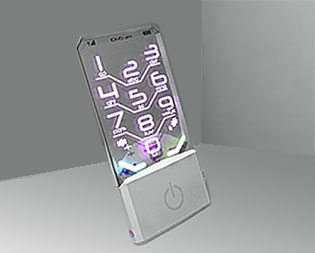
A common see through screen is almost like a transparent screen that is supported only by just a thin film of glass. The user of this side can use the side literally from any side and can watch it from any side too. This system has already been released by renowned companies like Planar Systems and Samsung .

The technology that is utilized by these devices is quite easy to understand. Earlier, in the working and the function part we had discussed about how various components for making the transparent devices were brought together,and here we are going to talk about how these components bond in accordance to the demands of the device.The common transparent device need a screen that should be multi-touch this is achieved with the help of two layers of crystal clear glass which hold a proper conductive layer, this allows these glass to produce their own light and are better known as OLED, which is an essential component of this technology. Finally, the gaps between the pixels get narrowed, which clears the cathodes that are present in the screen and thus allows the screen to be transparent. Though these types of screens had been expensive in the earlier days, but now with the work and impressive improvements by some of the leading manufactures, it has become affordable.
Sections