Electronics is my passion

Successive approximation Analog to Digital Converter circuit consists of four essential parts:
The SAR is initialized so that the most significant bit is logic 1 and all other bits are logic 0. This will force the DAC output to be Vref/2. Digital output of SAR is converted to analog output by internal digital to analog converter. If this voltage exceeds analog input Vin, then the comparator output resets the MSB bit in SAR. Conversely, if Vin is greater than DAC output, comparator output sets the MSB of the register.
In the next cycle, control logic then moves to the next bit down and set it to logic 1. Circuit does another comparison and same process is repeated all the way down to the LSB. Once this process done, the digital approximation of the sampled input analog voltage is obtained and is finally given as the output, by the SAR.
An N-bit SAR ADC requires N comparison periods. SAR will be ready for next conversion only after completing current conversion. Therefore, Successive Approximation ADC is comparatively slower than other ADC circuits.
Flash ADC is also called the parallel Analog to Digital converter. It is one of the fastest methods to convert an analog signal to a digital signal. A flash ADC is formed by a series of comparators, each one comparing the input signal to a unique reference voltage. Outputs of the comparators are connected to the inputs of an encoder, which then produces a binary output. Resolution of the ADC depends on the number of comparators used in the circuit. 2n-1 comparators are needed for n bit flash ADC conversion. Circuit of a two bit flash ADC with 3 comparators is shown in the figure.
Analog input is given as one of the input to each comparator. Second input of the comparator is set to different thresholds by the linear voltage ladder. Comparators indicate which of the thresholds have been exceeded. Output of each comparator produces logic high, only if, its input voltage (analog) is more than reference voltage given to it.
For a two bit ADC, an encoder converts the outputs of three comparators to a 2-bit digital value. A three-bit version would require 5 comparators. That is, for each additional output bit, the number of comparators required is increased by two. This is one major disadvantage of flash ADC.

Integrated analog-to-digital converters provide high resolution and noise rejection compared to other analog to digital converters. Resolution of integrated ADC depends on time, longer integration times allow for higher resolutions. But this reduces the speed of ADC and is one of the slowest ADCs. They are mostly used in applications like digital panel meters and digital multi-meters.
Unlike other types of ADCs, integrated-ADC use an op-amp circuit called an integrator to generate a saw tooth waveform instead of DAC with a ramped output. Integrated output is then compared against the reference voltage by a comparator.
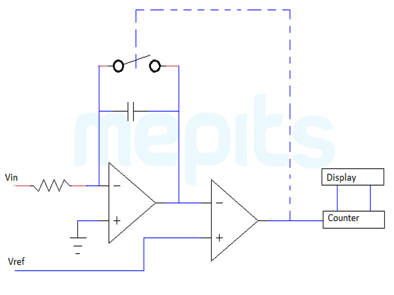
Single-slope ADC is the simplest form of an integrating ADC. Here, an unknown input voltage is integrated and the value is compared against a known reference value. Therefore, to guarantee measurement accuracy, the reference voltage used as one of input of the comparator must be accurate and stable.

Analog input is given to the input of op-amp integrator as shown in the figure. A continuously increasing ramp voltage is generated when a constant digital input is integrated. Integration is continued until ramp voltage is equal to reference voltage. Time duration for integrator to become equal to reference voltage is proportional to the magnitude of analog input. The counter is counting up at fixed rate of clock frequency during this period. When integration is completed, counter output gives digital value which is proportional to the magnitude of the input voltage.
When integrated output is equal to the reference voltage, comparator output allows capacitor discharge, making itself ready for next analog to digital conversion. Output of the comparator controls the switch across the capacitor to provide discharge path for the capacitor.
Accuracy of Single slope ADC depends on the tolerance of Resistor and Capacitor in the circuit. Thus a slight difference in each component's value can affect conversion result. Dual-slope integrating architecture is a solution to overcome this problem.
A dual-slope ADC, for a fixed amount of time holds and integrates an analog input voltage (Vin), then de-integrated for a variable amount of time. Any error introduced by a component value during the integrate cycle will be cancelled out during the de-integrate phase.

First analog input is integrated for a fixed duration and then de-integrated with reference input. The figure shows integrator output for three different inputs.

Discharge time is directly proportional to the magnitude of the input voltage. A digital counter is allowed to increment during this period. When discharge is completed, final count is the digital equivalent of analog input.
Sigma-delta converter offers high resolution, low power consumption, and low cost analog to digital conversion. A Basic sigma-delta ADC consists of an oversampling modulator followed by a digital/ decimation filter.

Figure shows a basic block diagram of sigma-delta analog to digital converter. An analog signal applied to the input of the converter is sampled multiple number of times. Each individual sample is then accumulated and averaged with the other input-signal samples by digital/decimation filter. Output data rate is hundred or more times slower than the sampling rate of modulator. While most converters have one sample rate, the Delta Sigma converter has two—the input sampling rate (fS) and the output data rate (fD)
Delta Sigma modulator
Delta-Sigma modulator is the heart of the Delta-Sigma Analog to Digital converter. It convert input analog signal into digital format. The modulator samples the input signal at a very high rate into a 1-bit stream and thus reduces noise at lower frequencies.
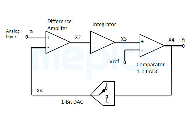
Figure shows the hardware architecture of a delta-sigma modulator, consists of an integrator, a comparator, and a negative-feedback loop with 1-bit digital-to-analog converter.

The inputs, sum of input signal and the negative output of the digital to analog converter is fed to integrator. A ramp signal is the output of the integrator whose slope output is proportional to the magnitude of its input signal. Output of the integrator is then compared with a reference signal to produce a 0 or 1.
Thus, the direction of the integrator ramp output is represented by each bit. Therefore, the bit stream after multiple iterations looks like the input signal after quantization. Ratio of the number of ones to zeros at the output of comparator is equivalent to the magnitude of input analog voltage. Therefore, if the output pulse train is averaged, we get input signal.
Binary output of the delta-sigma modulator is given to digital decimation block clocked at input sampling frequency. The signal is averaged by this block. In the frequency domain, averaging removes aliases and attenuates quantization noise as it has the effect of signal being low pass filtered.
Sections