I am an Electronics Engineer with keen interest in...More
Sections
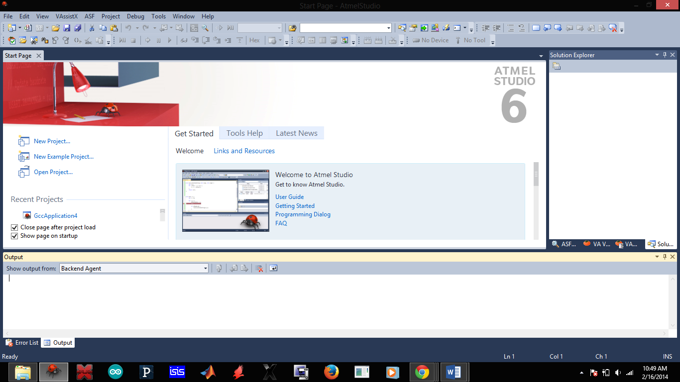
To start with Atmel Atmega series microcontrollers you will have to install Atmel Studio along with a suitable hardware programmer. The drivers of the programmer being used must also be installed. Once Atmel Studio is installed, on opening you will encounter a screen as shown below:

Click on New Project found on the left side. A new screen pops up:

Select GCC C Executable project. Any name can be given to your project. In the example, it is given as ‘Blink’. Also set the directory where the project is to be stored and click OK.
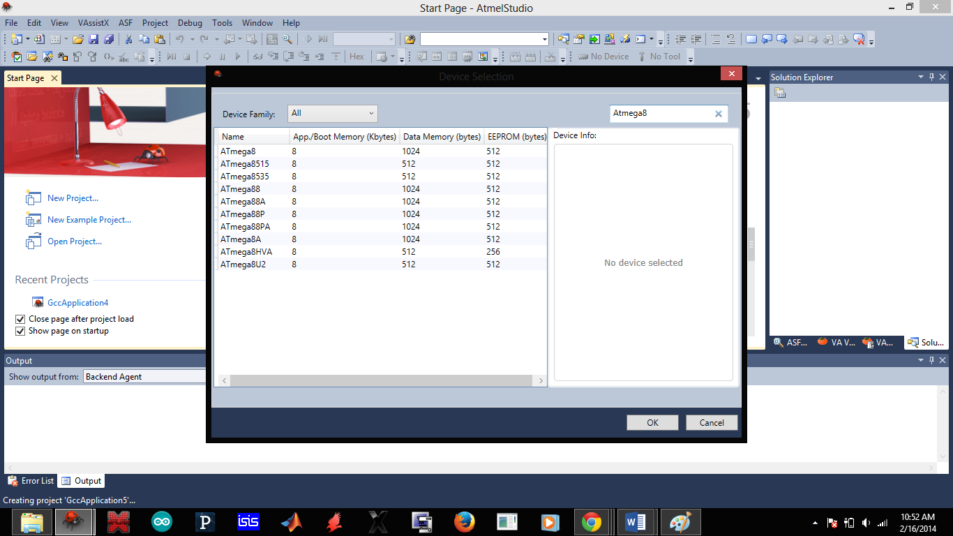
Next step is device selection. The microcontroller which is to be programmed must be selected. Here, Atmega8 has been chosen since that chip is being used.

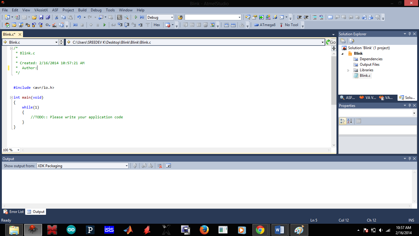
Finally, a window appears, as shown below, where the codes can be written:

By default a template code appears which can be replaced with your own code.
Once the code has been written, F7 must be pressed to compile the code and generate the hex files. Now to transfer the hex files to the chip, the hardware programmer must be connected to the computer. While doing so ensure that the microcontroller is connected to the programmer.
Goto Tools> Add Target. You’ll see the following:

Under serial port select the COM port to which your programmer is connected. This can be found from the device manager of your system. Click apply.
Now go to Tools>Device programming:

Under Device, select the chip that is to be programmed and click apply. This will connect your PC to the microcontroller. To program the chip, go to memories and browse for the hex file under flash. Do not mess with fuse and lock bits. Doing so without appropriate knowledge may render your chip useless. This will be found in the debug folder where you saved your project. Once you selected the file then click program. The LEDs on the programmer will flash appropriately and on completion you will get a message verifying flash…ok….
You are done with the basics of uploading a program to your chip.
The most widely used peripherals of any microcontroller are its digital input output ports. These allow the microcontroller to accept signals from the external environment and send signals to the same. There will be very few applications of microcontrollers which does not make use of the digital ports. The explanations will be based on Atmega8, an inexpensive chip from Atmel.
Atmega8 has two 8 bit wide digital ports B, D and a seven bit port C. All of them are capable of bidirectional data transfer (can be used as input or output). It is always good to refer to the datasheet which can be found here:
http://www.atmel.com/images/atmel-2486-8-bit-avr-microcontroller-atmega8_l_datasheet.pdf
Following is the pin diagram of Atmega8:

As shown in the figure, the pins PB0 (pin 14) to PB5 (pin 19) are 6 of the 8 bits of port B. Similarly, pins PC0-PC6 are the 7 bits of port C. Similar is the case with port D. Each of these bits can be set to be an input pin or an output independent of the status of the other bits in the port i.e. PB0 can be an input pin even when PB1 is an output pin. It has to be noted that most digital pins serve other purposes like MISO, MOSI etc. PC6 is the reset pin by default and cannot be used as a normal digital pin unless you modify the fuse settings.
Each port has a Data Direction Register (DDR) whose contents determine whether each bit of the port is an input or an output.
Consider PORTB. The corresponding Data Direction Register is DDRB. The pictorial representation is shown below:

Making a bit in the DDRB register to 0, sets the corresponding port bit to an input bit and making it a 1, sets the bit to an output. So if DDRB is 10101010, PB7, 5, 3,1 becomes outputs and 6,4,2,0 becomes input.

By default, all the digital pins of any AVR microcontroller is set to be an input on boot up. When a pin is defined to be an input, it can have anyone of the two states: the high impedance state (by default) or it can be set to 5V using the internal pull up resistor. High impedance state acts like an open switch (no electric potential is present at that pin).
Setting DDRB to 00000000 makes it an input port and will be in high impedance state by default. Now the pins PB0-7 is ready to accept voltage inputs. The maximum input voltage has to be limited to 5V.
PINB is the register which will contain the input values of port B.

If you connect a logic 1 to PB0 and PB7 pin while it is an input, PINB register becomes 10000001.
When a bit of a port is defined to be an output, it can have two states, ie, logic 1(5V) or logic 0(0v). The default value is logic 0. Once again taking digital port B for example, setting DDRB to 11111111 makes it an output.
The value of PORTB register determines the logic levels of the output pins. If PORTB is 11111111, all the pins PB0-7 will be at logic 1 and if it is 00000000, all the pins will be at logic 0.

One has to be careful not to provide any input to a pin which is configured as an output. Doing so may lead to short circuits and can damage the microcontroller.
Suppose DDRB is 00000000. This sets B to be an input. Now if PORTB is made to be 11110000 then pull up resistors will get activated in PB0-3 and PB4-7 which enters the high impedance state (tri state).
Now we are going to do something real with the I/O pins of Atmega8. We will be controlling an LED with the push of a button.

The easiest way to demonstrate the working of an input/output port is to control an led using push button. In the circuit, the anode of the LED is connected to PB0. The switch is connected to PC0. A pull down resistor keeps the value at ground. This ensures that the input pin is not affected by noise which may lead to erratic readings,when the button is pushed, it goes to 5V (logic 1).
 #include <avr/io.h>        //Basic I/O library for AVR microcontrollers
 int main(void)             // main function
 {
     int switch=0;          //stores switch status
     DDRB=0b00000001;       //PB0 is set to output
     DDRC=0b00000000;       //whole C register is set to input, but we use only PC0
     while(1)               //infinite loop
         {
         switch=PINC;       //contents of PINC register is stored
         PORTB=switch;      //contents of variable switch is copied to PORTB register
         }
 }
In the above piece of code, the DDR registers of B and C are set so that PB0 is output and PC0 is an input. The prefix ‘0b’ means that the following data is in binary. It is possible to do the same in hexadecimal by using ‘0x’ or in decimal system (no prefix is used). The infinite loop is used to keep the code running as long as the MCU is powered.
The status of the input register PINC, is 00000000 as long as the switch is not pushed and 00000001 when the switch is pushed. The value is stored to a temporary variable ‘switch’ which is then copied to the output register PORTB. The LED is connected to the 0th bit of PORTB. Hence, LED glows when the switch is pushed and goes off when released.
Now wire up the circuit and you are good to go. If you used the same code and circuit as above, you will see the LED light up when you press the push button and go off when you release it.
You can download the C file and the hex file from the documentation.
Sections